
 中文
中文

Why Are High-End Copper Alloys for Semiconductor Lead Frames So Difficult to Produce?
From Cu-Fe-P and Cu-Ni-Si to Ultra-Thin Copper Strips: Understanding the “Bottleneck” Copper Alloy Hidden Inside Chip Packaging
When people talk about semiconductor materials, they usually think first of silicon wafers, photoresists, electronic specialty gases, sputtering targets, packaging substrates, and bonding wires. However, a thin copper alloy strip is rarely mentioned.
Yet in the packaging of many integrated circuits (ICs), discrete devices, LEDs, sensors, and power semiconductor devices, the lead frame remains one of the most fundamental metallic structures.
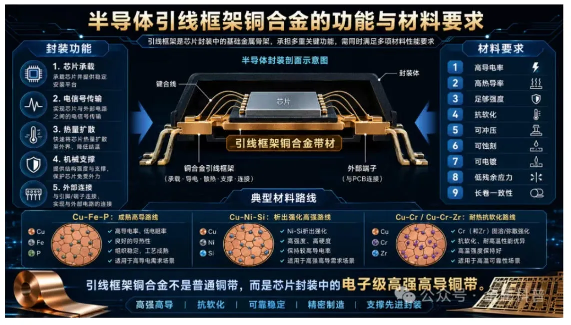
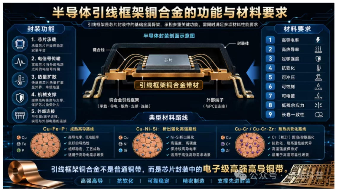
It is responsible not only for electrical signal transmission but also for chip support, heat dissipation, mechanical reinforcement, and external electrical connection. Lead frames are typically manufactured from thin sheets of copper, copper alloys, or Fe-Ni alloys, which are processed into fine structures through stamping or chemical etching. Different manufacturing methods impose different requirements on the strip material properties.
This is where the challenge begins: It may look like just a thin copper strip, but it cannot simply “conduct electricity.”
High-end lead frame copper strips must simultaneously satisfy multiple requirements:
| Required Property | Material Significance |
|---|---|
| High electrical conductivity / high thermal conductivity | Reduce electrical resistance and thermal resistance in packaging structures, supporting signal transmission and heat dissipation |
| Sufficient strength / resistance to softening | Ensure that thin leads and frames remain stable after stamping, packaging thermal processes, and thermal aging |
| Good stamping / etching / plating performance | Adapt to customers’ pattern processing, surface treatment, bonding, and soldering processes |
| Low residual stress / excellent flatness | Reduce package warpage, dimensional drift, and yield fluctuations during continuous production |
| Consistency throughout long coils | Ensure stable roll-to-roll production performance at customer facilities |
When all these requirements are combined, lead frame copper alloys are no longer ordinary copper strips. They become a typical class of electronic-grade, high-strength and high-conductivity copper alloy sheet and strip materials.
The real bottleneck is not only the chemical composition, but whether manufacturers can consistently produce high-end copper strips with the precise material state required for semiconductor packaging.
1. Why Can Chip Packaging Be Limited by a Thin Copper Strip?
Lead frames are not particularly eye-catching in semiconductor packaging. They are not like chips, which sit at the center of industry discussions, nor like packaging substrates, which are frequently discussed. However, for many packaging structures, lead frames remain the fundamental metal framework connecting chips with external circuits.
A single lead frame material must go through multiple stages, including coil feeding, stamping or etching, electroplating, die attachment, bonding, molding, trimming and forming, and reliability testing. Any problem occurring at any stage may result in reduced customer yield.
| Material or Process Variation | Problems That May Be Transferred to Customers |
|---|---|
| Insufficient strength | Thin leads deform after stamping, causing dimensional instability |
| Insufficient thermal conductivity | Increased device operating temperature and reduced thermal reliability |
| Poor surface condition | Unstable plating adhesion, poor bonding or soldering performance |
| Excessive residual stress | Package warpage and dimensional drift |
| Non-uniform precipitation structure | Variation in strength and electrical conductivity throughout the coil |
| Edge burrs and microcracks | Stamping cracks, abnormal etching, or packaging defects |
Therefore, lead frame copper alloys are not about making copper strips “as thin as possible.” Instead, the challenge is maintaining stable microstructure, performance, surface quality, and geometric accuracy under thin-gauge conditions.
Key conclusion: Producing one qualified sample in a laboratory is not difficult. The real challenge is consistently producing full coils of electronic-grade copper alloy strip that can pass packaging validation.

2. Why Can’t Pure Copper Be Used Directly?
Pure copper has excellent electrical conductivity and thermal conductivity, which naturally gives it advantages as a conventional conductor. However, a lead frame is not an ordinary wire.
It must first be rolled into thin strips and then undergo multiple processes, including stamping, etching, electroplating, die attachment, bonding, and molding. As semiconductor packaging continues to develop toward miniaturization, thinner structures, higher density, and higher power applications, material cross-sections become increasingly smaller, leads become finer, and packaging thermal processes become more complex. Under these conditions, the limitations of pure copper in terms of strength, softening resistance, and dimensional stability become increasingly apparent.
Pure copper can solve the problems of “electrical conductivity” and “thermal conductivity,” but it is difficult to simultaneously achieve sufficient thin-strip strength, stamping dimensional stability, resistance to softening after high-temperature packaging, deformation control for fine-pitch leads, and performance consistency during long-coil production.
Therefore, lead frame materials must transition from pure copper to copper alloys.
| Material System | Representative Materials | Core Advantages | Main Challenges |
|---|---|---|---|
| Cu-Fe-P system | C19400, KFC series | Mature and stable, balancing strength, conductivity, thermal conductivity, plating performance, and stamping capability | Limited strength ceiling |
| Cu-Ni-Si system | C7025, C7035 and other Corson alloys | Strong precipitation strengthening capability, suitable for high-strength thin strips and high-density packaging | Narrow process window and difficult strength-conductivity balance |
| Cu-Cr / Cu-Cr-Zr system | Cu-Cr, Cu-Cr-Zr | Better softening resistance and thermal stability | High requirements for thin-strip processing, surface quality, plating performance, and precision manufacturing |
C19400 is a typical Cu-Fe-P lead frame material. The Copper Development Association database lists C19400 as a material used for lead frames and highlights its characteristics including electrical conductivity, thermal conductivity, corrosion resistance, formability, and plating capability. Proterial also describes C194 as a high-strength, heat-resistant copper alloy with excellent plating performance, etching capability, and stamping properties, making it suitable for IC lead frames and LEDs.
Cu-Ni-Si represents a direction toward higher-strength materials. JX Advanced Metals describes C7025 as a precipitation-hardened Corson alloy, namely a Cu-Ni-Si alloy, and points out that it is widely used in connector terminals and lead frames.
This demonstrates that the selection logic for high-end lead frame copper alloys is not simply about “which material has the highest conductivity,” but rather about which material can maintain comprehensive stability throughout semiconductor packaging processes.
3. Why Are High Strength and High Conductivity Difficult to Achieve Simultaneously?
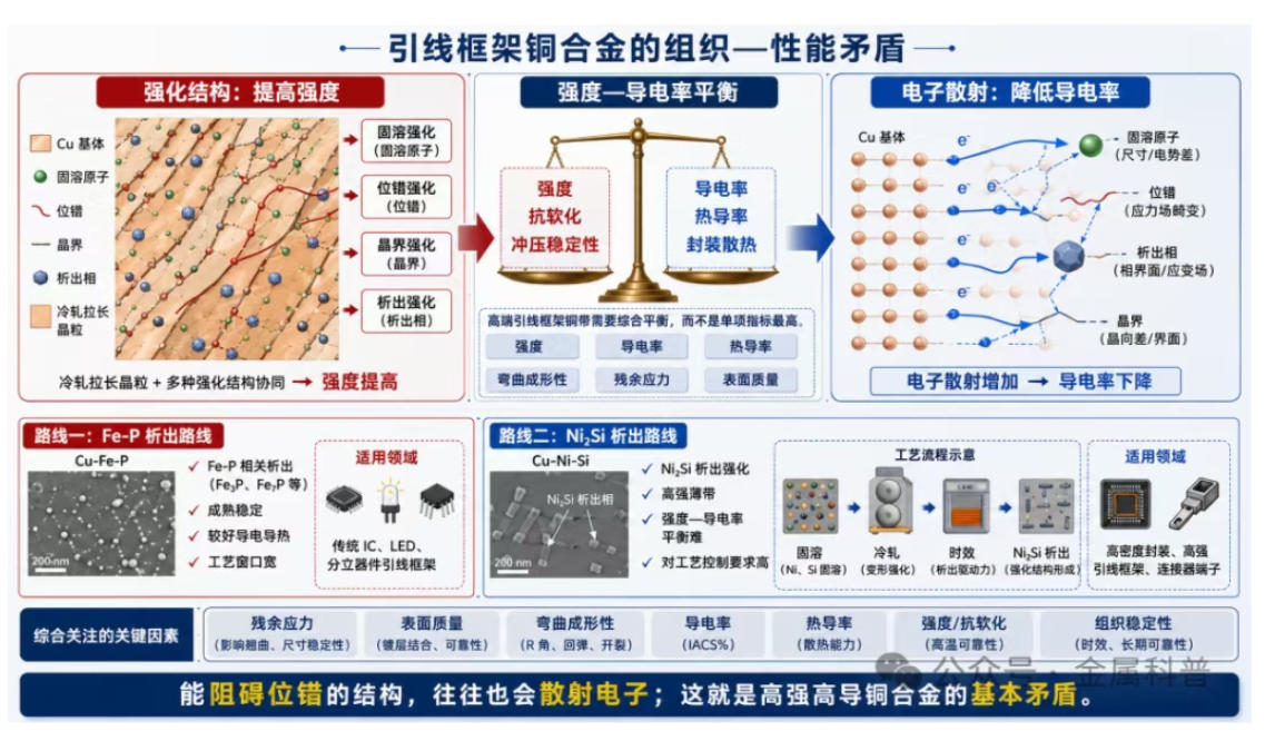
The most fundamental materials science challenge of lead frame copper alloys is the conflict between strengthening and electrical conductivity.
For copper-based materials, increasing strength usually relies on mechanisms such as solid solution atoms, dislocations, grain boundaries, precipitates, second-phase particles, texture, and deformation substructures. These structures can hinder dislocation movement, thereby increasing strength.
However, they also scatter electrons, resulting in reduced electrical conductivity. In other words, structures that can effectively block dislocation movement often also interfere with electron transport. This is the most basic materials science contradiction in high-strength, high-conductivity copper alloys.
For lead frame materials, it is impossible to simply maximize strength, nor is it practical to pursue the highest possible electrical conductivity alone. What material manufacturers truly need to achieve is a stable processing window that balances strength, electrical conductivity, thermal conductivity, stamping performance, etching performance, plating performance, softening resistance, and residual stress.
Cu-Ni-Si alloys are a typical example. A 2025 review on Cu-Ni-Si lead frame materials pointed out that Cu-Ni-Si alloys are considered a strong candidate system for IC lead frame applications. Strength and electrical conductivity are two core evaluation indicators, but they have an inverse relationship.
The basic processing logic of Cu-Ni-Si is: solution treatment → rapid cooling → cold rolling deformation → aging treatment → Ni₂Si-type precipitation strengthening → increased strength + partially recovered electrical conductivity.
A key point here is that electrical conductivity can partially recover after aging because part of the Ni and Si precipitates out from the Cu matrix. The matrix becomes “purified,” reducing electron scattering. However, if precipitation is insufficient, the strength will not be adequate; if precipitation is excessive or the precipitates coarsen, strength will decrease; if precipitation is non-uniform, the performance of the entire coil will fluctuate.
Therefore, the challenge of Cu-Ni-Si is not simply understanding “Ni₂Si precipitation strengthening,” but whether manufacturers can stably control the size, quantity, distribution of precipitates, and the solid-solution state of the matrix during continuous strip production.
The Cu-Fe-P system follows a similar principle. Although it is a more mature material system, it still requires control over Fe-P-related precipitation, deformation structure, and residual stress. For Cu-Fe-P lead frame alloys, studies have shown that dislocations, precipitates, and texture characteristics can all affect residual stress states, while residual stress itself influences subsequent warpage and processing stability.
Therefore, high-end lead frame copper alloys are not merely a matter of chemical composition, but a typical coupled problem involving composition, microstructure, texture, residual stress, and customer processing performance.
4. Why Does a Qualified Sample Not Mean High-End Long-Coil Mass Production Is Achievable?
One of the most common misunderstandings about this type of material is that many people assume a material is successfully developed as long as its sample strength and conductivity meet requirements. In reality, this is not the case.
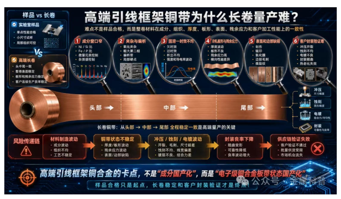
For lead frame copper alloys, single-point performance data has limited significance. Customers use continuous coils, and what they truly care about is the stability of the entire coil.
| Stability Requirements for High-End Long Coils | Impact on Customer Packaging Production Lines |
|---|---|
| Consistent performance from the beginning, middle, and end of the coil | Reduce parameter drift and yield fluctuations during continuous production |
| Consistent thickness in both transverse and longitudinal directions | Ensure dimensional stability during stamping, etching, and assembly |
| No periodic scratches or roll marks on the surface | Improve reliability of plating, bonding, and packaging |
| Stable flatness | Reduce coil feeding problems and package warpage |
| Controlled edge burrs after slitting | Reduce risks of stamping cracks, short circuits, and burr-related defects |
| Low and uniformly distributed residual stress | Reduce dimensional drift, warpage, and subsequent deformation |
This is fundamentally different from ordinary copper strips. Conventional materials may tolerate a certain range of performance variation, but high-end lead frame copper strip can transfer even minor fluctuations directly to packaging production lines.
For example, crystal defects introduced during rolling, such as dislocations, vacancies, and stacking faults, can affect residual stress, while residual stress further influences dimensional stability and warpage behavior. Research on lead frame copper alloys indicates that rolling and aging are commonly involved in their manufacturing processes, and rolling introduces a large number of crystal defects that are closely related to residual stress.
Therefore, the challenge of high-end lead frame copper strips is not a single performance indicator, but the stable coordination among a series of interconnected properties.
5. Problem 1: Narrow Composition Window
Different lead frame copper alloys have different key requirements for composition control. For Cu-Ni-Si alloys, the Ni/Si ratio is particularly critical. Ni and Si need to form effective Ni₂Si-type precipitates. If Ni or Si content is excessive, it may increase residual solute elements, reduce electrical conductivity, or generate undesirable second phases.
For Cu-Fe-P alloys, the ratio of Fe and P also affects precipitation behavior, electrical conductivity, and thermal stability.
In addition, impurities such as Pb, Bi, S, O, As, and Sb must be strictly controlled. Although these elements exist at very low levels, they may significantly affect hot processing, cold rolling, stamping, electroplating, and reliability performance. High-end electronic copper strips cannot be evaluated only by the main element composition range; impurity profiles, furnace-to-furnace consistency, and long-term batch stability must also be considered.
6. Problem 2: Difficult Control of Melting Cleanliness and Segregation
Lead frame copper alloys are highly sensitive to inclusions and segregation.
Oxide inclusions, coarse second phases, composition segregation, and porosity defects in cast billets are difficult to completely eliminate in subsequent processes. Even after hot rolling and cold rolling, these problems may appear as surface defects, edge cracks, local hard spots, uneven etching, or stamping cracks.
For Cu-Ni-Si alloys, if Ni and Si are unevenly distributed, the subsequent solution treatment and aging response will also become non-uniform. Some regions may achieve sufficient precipitation strengthening, while others may experience insufficient precipitation, ultimately resulting in performance fluctuations within the same coil.
For electronic-grade strip materials, the cast billet is not merely an intermediate product; it is the starting point that determines final production yield.
7. Problem 3: Narrow Solution Treatment–Cold Rolling–Aging Processing Window

8. Problem 4: Challenges in Precision Cold Rolling and Flatness Control
Lead frame copper strips typically require thin gauges, long-coil production, and high surface quality. Cold rolling is not only a thickness reduction process but also a process for controlling microstructure and stress. Rolling introduces dislocations, texture, and residual stress, and it also affects subsequent aging behavior and customers’ forming performance.
The challenges of high-end cold rolling include tight thickness tolerances, stable flatness, the absence of roll marks, scratches, and dents on the surface, prevention of microcracks at the edges, stable coil tension, minimized transverse property variations, and controlled residual stress levels.
These issues may appear to be merely “strip processing problems” within the material manufacturer, but at the customer’s side they can become stamping deformation, uneven etching, poor plating performance, package warpage, and reduced yield during continuous production.
9. Problem 5: Surface Quality Determines Plating, Etching, and Bonding Performance
Lead frame copper strips must be compatible with subsequent surface treatment and packaging processes. In Proterial’s description of C194 lead frame alloys, besides high strength and heat resistance, it also specifically emphasizes plating performance, etching capability, and stamping performance. This indicates that for lead frame materials, surface processing compatibility itself is an important part of material value.
Surface-related issues include oil contamination residues, oxide films, micro-scratches, copper powder and rolling residues, roll marks, color variations, roughness fluctuations, localized corrosion, and slitting burrs.
These defects may affect plating layer adhesion, etching uniformity, bonding stability, and packaging reliability. Therefore, high-end lead frame copper strips cannot be evaluated only by microstructure; surface condition must also be carefully controlled.
10. Problem 6: Long Customer Validation Cycles
The final qualification of lead frame copper alloys is not determined solely by the material manufacturer, but by validation on the customer’s packaging production line. Material suppliers may have already tested composition, tensile strength, hardness, electrical conductivity, metallographic structure, and surface quality.
However, customers still need to further validate stamping burrs, etching accuracy, plating adhesion, chip attachment, bonding stability, molding warpage, thermal cycling, high-temperature aging, solderability, contact reliability, and continuous mass production yield.
Wieland’s semiconductor packaging strip materials documentation also points out that lead frames for ICs and discrete devices are typically manufactured through stamping or etching, and different processing methods require different strip properties. Therefore, suppliers need to provide strip qualities optimized for different manufacturing processes.

11. Where Exactly Is the “Bottleneck” of This Type of Material?
Semiconductor lead frame copper alloys are not the type of critical material that easily attracts public attention. Unlike photoresists, electronic specialty gases, or silicon wafers, they naturally receive less attention in industry discussions. However, from the perspective of the materials industry, they truly test a country’s manufacturing capability in high-end copper alloy sheets and strips.
The challenge is not whether materials such as C19400, C7025, or Cu-Ni-Si grades exist, nor whether it is possible to produce a high-strength, high-conductivity sample in a laboratory.
The real challenge is whether manufacturers can stably produce electronic-grade copper alloy strips that are thin, flat, clean, strong, conductive, heat-resistant, suitable for stamping, suitable for etching, suitable for electroplating, with low residual stress, and with consistent performance throughout long coils.
This is the true industrial bottleneck of lead frame copper alloys.
Conclusion: The First Article Only Answers “Why Is It Difficult?”
If oxygen-free copper rods with O < 5 ppm test the capability of low-oxygen melt control systems, then high-end lead frame copper alloys test the manufacturing capability of electronic-grade copper alloy sheet and strip systems.
It is not simply a matter of “rolling copper alloy thinner.” Instead, the final material state is jointly determined by composition design, melting, casting, homogenization, hot rolling, cold rolling, solution treatment, aging, finishing, cleaning, slitting, inspection, and customer packaging validation.
Jintian Copper produces C194 and C192 lead frame copper strips. Welcome to contact us for consultation. Tel: 0574-83005999, WeChat: 18057437999.
References and Data Sources
[1] Copper Development Association. UNS C19400 Alloy Database.
[2] Proterial. Copper alloy strip for semiconductor lead frames.
[3] JX Advanced Metals. C7025 – Corson Alloy for lead frames and connectors.
[4] JX Advanced Metals. Corson Alloys.
[5] Yan H., et al. Research Progress of Cu-Ni-Si Series Alloys for Lead Frame Materials. Coatings, 2025.
[6] Yang K., et al. Recent development of advanced precipitation-strengthened Cu alloys. Progress in Materials Science, 2023.
[7] Nam H. M., et al. Precipitation strengthening of Cu-Ni-Si-based alloys. Journal of Materials Research and Technology, 2023.
[8] Cao T., et al. Evolution of microstructure and residual stress for a lead-frame Cu-Fe-P alloy. Journal of Alloys and Compounds, 2023.
[9] Wang B., et al. Microstructure and residual stress gradient evolution in rolled lead-frame copper alloy strips. Journal of Alloys and Compounds, 2024.
[10] Liao W., et al. Effect and mechanism of solidified microstructure on residual stress and deformation behavior of Cu-Ni-Si alloy. 2022.
[11] Wieland. Strip for semiconductor packages.
[12] Mitsubishi Materials. TAMAC Series Cu-Fe Alloy / TAMAC194.
[13] Precision Micro. The economic manufacture of lead frames: chemical etching and stamping.
[14] ASM International. ASM Specialty Handbook: Copper and Copper Alloys.
[15] ASM Handbook. Properties and Selection: Nonferrous Alloys and Special-Purpose Materials.
[16] NIST. Copper and Copper Alloys, NIST Monograph 177.
[17] Furukawa Electric. Technical trends in copper alloys and plating for automotive terminals.
[18] Kobe Steel. Technical trends in copper alloys and plating for automotive terminals.
[19] Springer Handbook / lead frame packaging materials related chapters.
[20] ScienceDirect Topics. Lead Frame / semiconductor packaging overview.
[21] GB/T and ASTM related copper alloy strip specifications for electronic applications.
[22] IEC and JEDEC related semiconductor package reliability and thermal cycling test references
-
Tel:
-
E-mail:
-
Address:
No.1 Chengxi West Road, Cicheng, Ningbo, China
-

Ms.Yu
-

Ms.Sun