
 中文
中文

Tinned Copper Wire: Why Is It So Widely Used—and Why Does It Sometimes Become Difficult to Solder?
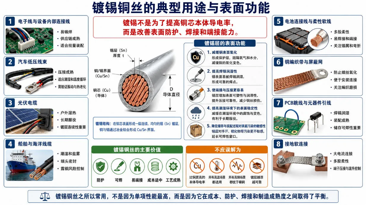
Note: This article discusses the material principles, applications, performance limits, and inspection logic of tinned copper wire. It does not disclose electrolyte compositions, plating temperatures, current densities, immersion speeds, or post-treatment parameters that could be directly replicated in manufacturing. The discussion of tin whiskers mainly references studies on electronic component leads, connectors, and electroplated tin coatings to explain the underlying risk mechanisms. These findings should not be interpreted as meaning that all tinned copper wires will develop tin whiskers.
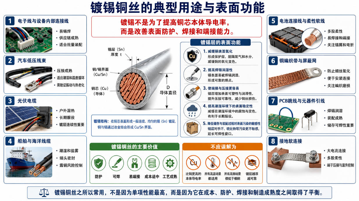
Tinned copper wire is one of the most widely used surface-treated copper conductors. Although it does not carry the same "premium" reputation as silver-plated copper wire, it is extensively used in equipment internal wiring, automotive wiring harnesses, photovoltaic cables, marine cables, flexible power connectors, copper braided straps, and PCB lead wires. Manufacturers choose tin plating not because it improves the intrinsic conductivity of the copper core, but because it makes copper easier to store, terminate, solder, and use in humid environments.
The real question is this: if tin plating is intended to improve solderability, why do some wires solder perfectly when newly manufactured but exhibit significantly slower wetting after storage? If the tin layer is designed to protect copper, why can prolonged exposure to elevated temperatures, stranding, and long-term service eventually lead to copper-tin intermetallic compounds, flaking, exposed copper, or even the potential risk of tin whiskers?
ASTM B33 covers soft annealed tinned copper wire for electrical purposes, specifying requirements for resistivity, tensile properties, dimensions, and coating continuity [1]. ASTM B965 is specifically intended for high-performance electroplated tinned annealed copper wire where solderability is a primary requirement, emphasizing coating thickness, coating continuity, and solderability testing in addition to electrical and mechanical properties [2]. These standards demonstrate that "having tin on the surface" and "maintaining long-term solderability" represent two different levels of performance.
The real value of tinned copper wire is not a brighter surface, but its ability to preserve protection, solderability, and reliable termination throughout the product lifecycle.
1. What Is Tinned Copper Wire? The Copper Core Conducts Electricity, While the Tin Layer Makes Copper Easier to Use
Tinned copper wire typically consists of a copper conductor coated with an outer layer of tin or a tin-based finish. The copper core provides electrical conductivity, mechanical strength, flexibility, and drawing performance, while the tin layer forms the outermost surface exposed to air, insulation extrusion, terminals, solder, moisture, and contaminants.
Tin has significantly lower electrical conductivity than copper, so the purpose of tin plating is generally not to improve the overall conductivity of the conductor. Instead, its advantages mainly come from three aspects:
-
Tin surfaces readily form metallurgical bonds with common solders.
-
The tin layer delays direct oxidation and discoloration of the copper surface.
-
A uniform tin surface helps stabilize soldering and electrical contact processes during stranding, braiding, and terminal assembly.
However, this surface is not static. Tin oxidizes, copper and tin diffuse into one another, and the coating gradually becomes thinner or develops cracks during wire drawing, stranding, and repeated bending. In other words, the performance of tinned copper wire depends on the combined interaction of the copper core, tin coating, copper-tin interface, and subsequent manufacturing processes.
2. Where Is Tinned Copper Wire Used? Different Applications Require Different Functional Priorities
| Typical Applications | Why Tinned Copper Wire Is Used | Application Challenges Addressed |
|---|---|---|
| Internal Connections in Electronic Devices | Easy soldering and assembly, reducing oxidation and improving storage stability | Storage reliability, wire oxidation, solder joint reliability |
| Automotive Wiring Harnesses | Suitable for high-temperature, vibration, and humid environments | Corrosion resistance, vibration, heat resistance, temperature differences in engine compartments |
| Photovoltaic and Outdoor Cables | Withstands long-term outdoor exposure, temperature variations, and connection requirements | Aging, UV radiation, oxidation, insulation compatibility |
| Ship and Marine Cables | Resistant to moisture and corrosion in marine environments | Salt spray, moisture ingress, corrosion resistance, mechanical damage |
| Oilfield Cables and Flexible Cables | Multi-strand structures provide flexibility while maintaining conductivity | Bending fatigue, mechanical wear, compression resistance |
| Tinned Copper Braids and Shielding Mesh | Fine strands, large surface area, used for shielding and grounding connections | Shielding performance, flexibility, connection consistency |
| PCB Wires and Component Leads | Facilitates soldering and improves manufacturing efficiency | Long-term solder joint reliability, aging, surface contamination |
| Industrial Control Systems and Sensors | Balances cost and reliability, suitable for stable supply chain applications | Temperature fluctuations, soldering processes, surface condition after processing |
| Grounding Connections | Multi-strand structure, suitable for installation connections and humid environments | High-current conduction, compression and soldering connection reliability |
The common characteristic among these applications is not the need for higher electrical conductivity, but the need for copper conductors to remain solderable, connectable, and surface-stable throughout manufacturing and service. The industrial value of tinned copper wire lies more in its manufacturing compatibility than in achieving a single peak material property.
3. Why Hot-Dip Tin Plating and Electroplated Tin Cannot Be Described by a Single Term
The two most common industrial tin-plating methods are hot-dip tin plating and electroplated tin. Both produce a tin-coated surface, but they differ in thermal history, coating thickness control, surface morphology, and copper-tin interfacial structure.
| Comparison Item | Hot-Dip Tinning | Electroplated Tinning |
|---|---|---|
| Coating Formation | Copper wire passes through molten tin or tin alloy to form a coating layer | Coating layer is formed through an electrochemical deposition process |
| Common Characteristics | The coating is relatively thicker, and the process is significantly affected by temperature and line speed | Thickness and surface quality are easier to control, making it suitable for fine wires and precision products |
| Copper Reaction | An obvious intermetallic reaction occurs during the formation process | Initial interface reaction is relatively weak, but continuous diffusion and aging may still occur over time |
| Main Risks | Tin whiskers, local uneven coating, dimensional fluctuations, and thermal effects | Pinholes, residual stress, thin coating, and sensitivity to wire diameter |
| Common Applications | Traditional wires, larger specifications, and products requiring continuous coating | Electronic wires, fine wires, and high-performance conductive materials |
The comparison presented here reflects only typical characteristics. It does not mean that every hot-dip coating is thick or every electroplated coating is thin. The final product characteristics are determined by the finished wire diameter, whether additional drawing follows plating, subsequent heat treatment, stranding, and insulation processing. For purchasers, asking whether the product is hot-dip or electroplated is only the first step. More importantly, they should verify the minimum local coating thickness, coating continuity, and solderability throughout the intended service life.
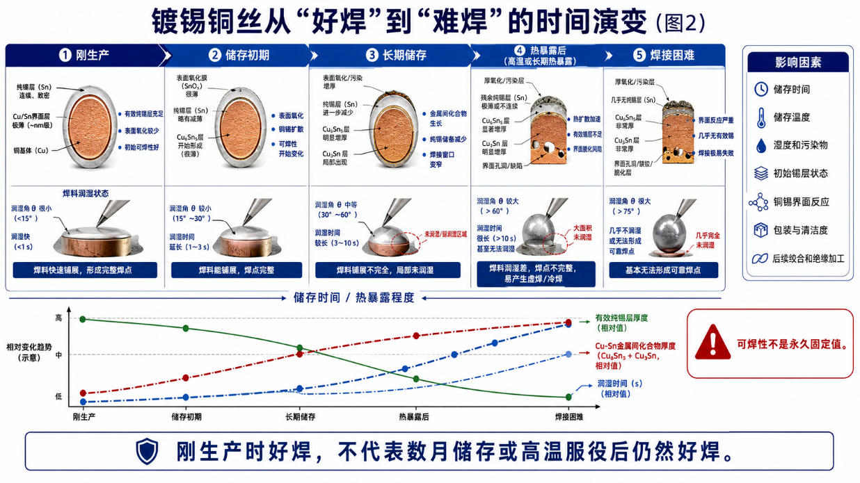
4. Why Is Newly Produced Wire Easy to Solder but Sometimes Difficult to Solder After Storage?
Successful soldering is not simply a matter of solder sticking to the tin surface. A reliable metallurgical bond requires the flux to remove surface oxides, molten solder to wet the tin layer, and appropriate copper-tin intermetallic compounds to form at the interface. Copper-tin reactions are essential for solder joint formation, yet excessive intermetallic growth eventually consumes the free tin layer and alters the interface.
Within the copper-tin system, the most common intermetallic compounds are Cu₆Sn₅ near the tin side and Cu₃Sn closer to the copper substrate. Studies conducted by NIST on multiple tin-based solder/copper interfaces show that thermal aging continuously increases the thickness of intermetallic compound layers [20–21]. From the perspective of wire products, this means that the free tin layer present at shipment gradually becomes thinner over time as interfacial reactions continue during storage and elevated-temperature exposure.
Declining solderability is usually caused by several factors acting together:
-
Oxidation, contamination, or volatile packaging residues make it more difficult for flux to remove surface films.
-
Copper diffuses into the tin coating, allowing Cu₆Sn₅ and Cu₃Sn layers to continue growing while consuming the free tin layer.
-
Thin coating areas or coating pores expose copper earlier, accelerating oxidation.
-
High-temperature insulation extrusion, baking, transportation, or storage accelerates diffusion and surface evolution.
-
Soldering temperatures and flux systems may no longer match the aged surface condition.
Therefore, solderability is not a property that remains permanently valid after a single factory inspection. The reason ASTM B965 specifically includes solderability as an independent requirement is precisely because long-term solderability cannot be guaranteed by appearance or electrical resistivity alone [2–3].
The transition from "easy to solder" to "difficult to solder" is usually not caused by the sudden disappearance of tin, but by the gradual shift in the balance among the free tin layer, surface oxide film, and copper-tin intermetallic compounds.
5. A Thicker Tin Layer Is Not Always Better—The Real Challenge Is Maintaining Coating Continuity After Processing
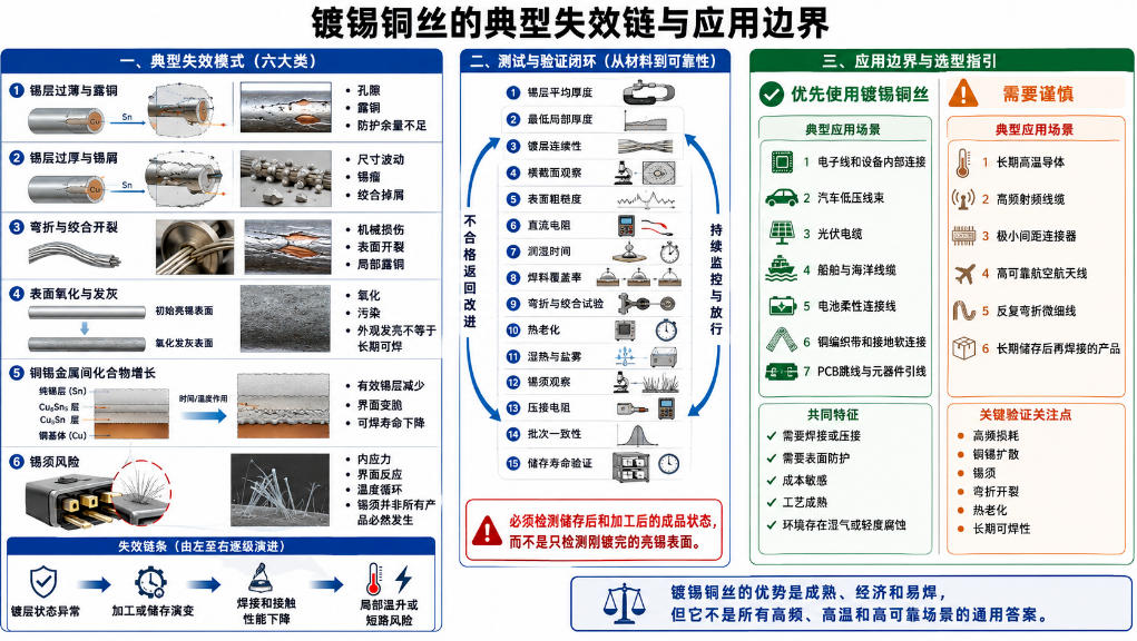
When the tin coating is too thin, there is little tolerance for pores, exposed copper, or localized thin regions. Drawing, stranding, and repeated bending make coating failure more likely. During storage or thermal exposure, the free tin layer is also consumed more rapidly by interfacial reactions.
Excessively thick tin coatings create another set of challenges. They may increase finished wire diameter variation and roundness deviation, generate tin flakes or localized buildup during fine-wire stranding, promote coating cracks because the thicker tin layer deforms differently from the copper core during repeated flexing, and increase both material cost and the amount of tin available for continued copper-tin reactions.
One of the most common misconceptions is evaluating products only by average coating thickness or surface brightness. A compliant average thickness does not eliminate locally thin regions around the wire circumference, and a bright surface does not guarantee good solderability after months of storage.
A meaningful evaluation should simultaneously examine minimum local coating thickness, coating continuity, post-stranding surface condition, and solderability after thermal aging.
6. Why Tin Whiskers Deserve Attention—but Not Every Tinned Copper Wire Should Be Considered High Risk
Tin whiskers are slender metallic crystals that spontaneously grow from tin or tin-rich surfaces. They may bridge adjacent conductors and cause electrical short circuits, making them an important reliability concern in high-density electronics, aerospace systems, and maintenance-free equipment. NASA, JEDEC, and IPC have all published technical guidance on tin whisker mechanisms, testing, and mitigation [10–16].
Current research generally agrees that compressive stress and stress relaxation are major driving forces behind tin whisker growth. These stresses may originate from electroplating processes, Cu₆Sn₅ formation, thermal cycling, mechanical bending, or external loading. Fukuda et al. observed that mechanically bent regions produced denser and longer tin whiskers [17], while Horváth et al. showed that grain structure, annealing conditions, and copper diffusion significantly influence whisker initiation and morphology [18–19].
However, it is important to distinguish between wire products and electronic component coatings. Connector terminals, component leads, and sheet-metal coatings typically involve electroplated tin on rigid substrates whose internal stresses, coating thicknesses, bending conditions, and conductor spacing differ significantly from stranded tinned copper wire.
Studies on tin whiskers help explain potential mechanisms, but they should not be interpreted as evidence that all tinned copper wires will inevitably grow whiskers.
For ordinary power cables and wiring harnesses with relatively large conductor spacing, tin whiskers are not necessarily the dominant reliability concern. For extremely fine-pitch connectors, aerospace electronics, sealed equipment, and other high-reliability applications, coating type, residual stress, temperature-humidity cycling, and conductor spacing should be specifically evaluated.
7. When Is Tin Plating Appropriate, and When Should Another Surface Finish Be Considered?
| Application Scenario | Value and Limitations of Tinned Copper Wire | Evaluation Criteria |
|---|---|---|
| Low-Voltage Electronic Wires and Equipment | Solderable, economical, easy to process, and convenient for assembly | Give priority to evaluating tinned copper wire |
| Automotive Low-Voltage Wiring Harnesses | Provides reliable soldering performance and adapts to temperature fluctuations and vibration environments | Verify based on environmental conditions and connection methods |
| Ship, Outdoor, and Humid Environment Cables | Enhances surface protection and facilitates soldering and connection processes | Evaluate based on cable structure, terminal design, and shielding requirements |
| Multi-Strand Flexible Wires and Braided Straps | Fine strands provide flexibility and support shielding and grounding connections | Focus on fatigue resistance, bending performance, and connection durability |
| Long-Term Current-Carrying Conductors | Copper diffusion and intermetallic growth may accelerate over time | Evaluate based on application duration and possible aging mechanisms |
| High-Frequency Signal Conductors | Surface conductivity and soldering characteristics may affect signal quality | Do not use tinned copper wire as the only basis for material selection |
| Extremely Fine Wires and Micro Connections | Sensitive to coating thickness and interface stability | Requires verification of coating process and long-term reliability |
| Products Requiring Long-Term Storage or Shipment | Surface and interface properties may change over time | Requires evaluation of storage conditions and aging behavior |
The greatest advantages of tinned copper wire are its mature manufacturing technology, cost effectiveness, and compatibility with large-scale production—not its ability to outperform bare copper, silver plating, or nickel plating in every performance category. High-frequency applications, elevated-temperature environments, and ultra-high reliability systems often require a different surface finish, while cost-sensitive, low-frequency products do not necessarily benefit from selecting a more expensive coating simply because it appears more advanced.
8. At Least Nine Items Should Be Specified During Procurement and Inspection
-
Copper grade, temper, finished single-wire diameter, and dimensional tolerance.
-
Hot-dip tin plating, electroplated tin, or other tin-based surface finish.
-
Whether plating is applied to the finished wire or followed by additional drawing, annealing, stranding, or braiding.
-
Definition of average coating thickness, minimum local coating thickness, or coating weight.
-
Requirements for coating continuity, exposed copper, tin nodules, tin flakes, and surface contamination.
-
DC resistance, tensile strength, elongation, and bending performance.
-
Initial solderability and solderability after thermal aging, steam aging, or storage.
-
Compatibility with crimping, soldering, insulation extrusion, and end sealing.
-
Whether high-reliability products require solder joint validation, temperature-humidity cycling, and batch traceability.
The most important consideration is to clearly define the test condition, and select tinned copper wire suppliers that can provide consistent coating quality and reliable performance verification.
A plated parent wire meeting specifications does not necessarily mean the finished drawn or stranded wire will also comply. Likewise, a wire that solders well immediately after production may no longer solder adequately after six months of customer storage.
Inspection requirements should therefore be designed to reflect the actual service condition of the finished product as closely as possible.
9. Conclusion: Tinned Copper Wire May Be Ordinary, but It Demands Long-Term Surface Management
Tinned copper wire is widely used not because tin conducts electricity better than copper, but because it provides a practical balance among solderability, surface protection, manufacturing compatibility, and cost. For countless electronic wires, wiring harnesses, and flexible electrical connections, this balance is often more valuable than pursuing a single extreme material property.
However, the tin coating is not a permanent protective shell. It oxidizes, reacts with copper to form Cu₆Sn₅ and Cu₃Sn, becomes thinner or flakes during drawing, stranding, and bending, and may even develop tin whiskers under specific combinations of stress and environmental conditions.
Ultimately, long-term reliability depends not on how bright the surface appears immediately after production, but on whether sufficient free tin and continuous surface coverage remain after storage, thermal exposure, termination, and years of service.
Therefore, purchasing tinned copper wire should involve much more than asking whether the conductor is tin-plated.
Additional questions should include:
-
What tin-plating process is used?
-
What is the minimum local coating thickness after final processing?
-
How long will solderability be maintained during storage?
-
How much will the intermetallic layer grow after thermal exposure?
-
Will exposed copper or coating flaking occur after repeated bending or stranding?
High-quality tinned copper wire is not defined by its silver-white appearance at shipment, but by a predictable and reliable surface condition throughout manufacturing, storage, and final assembly.
The next article in this series will discuss:
Enamelled Copper Wire: How Can an Insulation Layer Only a Few Micrometers Thick Determine Motor Lifetime?
References and Standards
The following references are used to support discussions of tinned copper wire standards, service temperature, solderability, copper-tin intermetallic compounds, and tin whisker risks. Because the sample types and application conditions in the tin whisker literature vary considerably, care should be taken to understand the applicable boundaries of each reference when interpreting the findings.
[1] ASTM International. ASTM B33-10(2020)e1, Standard Specification for Tin-Coated Soft or Annealed Copper Wire for Electrical Purposes.
[2] ASTM International. ASTM B965-09(2026), Standard Specification for High Performance Tin-Coated Annealed Copper Wire Intended for Electrical and Electronic Application for Solderability.
[3] ASTM International. ASTM B973-10(2020)e1, Standard Specification for Tin-Coated Braid and Ribbon Flat Copper Wire Intended for Use in Electronic Application.
[4] SAE International. AS22759E, Wire, Electrical, Fluoropolymer-Insulated, Copper or Copper Alloy, 2024.
[5] SAE International. AS22759/18A, Wire, Electrical, Extruded ETFE, Light Weight, Tin-Coated Copper Conductor, 600 V, 150 °C, 2019.
[6] SAE International. AS22759/85C, Wire, Electrical, PTFE/Polyimide Insulated, Normal Weight, Tin-Coated Copper Conductor, 150 °C, 600 V.
[7] SAE International. AS50861/7A, Wire, Electrical, PVC Insulated, Polyamide Jacket, Tin-Coated Copper Conductor, 600 V, 105 °C.
[8] SAE International. AS81044, Wire, Electrical, Crosslinked Polyalkene/Polymer Insulated, Copper or Copper Alloy Conductors.
[9] SAE International. AS4372C, Performance Requirements for Wire, Electric, Insulated, Copper or Copper Alloy.
[10] JEDEC. JESD201, Environmental Acceptance Requirements for Tin Whisker Susceptibility of Tin and Tin Alloy Surface Finishes.
[11] JEDEC. JESD22-A121A, Test Method for Measuring Whisker Growth on Tin and Tin Alloy Surface Finishes.
[12] IPC/JEDEC. JP002, Current Tin Whiskers Theory and Mitigation Practices Guideline.
[13] NASA Electronic Parts and Packaging Program. Basic Information on Tin Whiskers, 2019.
[14] Brusse J A, Ewell G J, Siplon J P. Tin Whiskers: Attributes and Mitigation. NASA NEPP Technical Paper, 2002.
[15] Brusse J A. Tin Whiskers: Revisiting an Old Problem. NASA NEPP, 1998.
[16] McDowell C M E. Tin Whiskers: A Case Study. NASA Goddard Space Flight Center, 1992.
[17] Fukuda Y, Osterman M, Pecht M. The impact of electrical current, mechanical bending, and thermal annealing on tin whisker growth. Microelectronics Reliability, 2007, 47(1): 88-92. doi:10.1016/j.microrel.2006.04.011.
[18] Horváth B, Illés B, Shinohara T, Harsányi G. Whisker growth on annealed and recrystallized tin platings. Thin Solid Films, 2012, 520(17): 5733-5740. doi:10.1016/j.tsf.2012.03.130.
[19] Horváth B. Influence of copper diffusion on the shape of whiskers grown on bright tin layers. Microelectronics Reliability, 2013, 53(7): 1009-1020. doi:10.1016/j.microrel.2013.03.008.
[20] Madeni J C, et al. Intermetallics Formation and Growth at the Interface of Tin-Based Solder Alloys and Copper Substrates. NIST, 2003.
[21] NIST. Test Procedures for Developing Solder Data, NIST Special Publication 960-8.
[22] Choi W K, Kang S K, Shih D Y. A study of the effects of solder volume on the interfacial reactions in solder joints using the differential scanning calorimetry technique. Journal of Electronic Materials, 2002, 31: 1283-1291. doi:10.1007/s11664-002-0022-x.
[23] Boettinger W J, Johnson C E, Bendersky L A, Moon K W, Williams M E, Stafford G R. Whisker and hillock formation on Sn, Sn-Cu and Sn-Pb electrodeposits. Acta Materialia, 2005, 53(19): 5033-5050. doi:10.1016/j.actamat.2005.07.016.
[24] Lee B Z, Lee D N. Spontaneous growth mechanism of tin whiskers. Acta Materialia, 1998, 46: 3701-3714. doi:10.1016/S1359-6454(98)00045-7.
[25] Howard H P, Cheng J, Vianco P T, Li J C M. Interface flow mechanism for tin whisker growth. Acta Materialia, 2011, 59: 1957-1963. doi:10.1016/j.actamat.2010.11.061.
[26] Tu K N. Interdiffusion and reaction in bimetallic Cu-Sn thin films. Acta Metallurgica, 1973, 21: 347-354.
[27] Tu K N, Thompson R D. Kinetics of interfacial reaction in bimetallic Cu-Sn thin films. Acta Metallurgica, 1982, 30: 947-952.
[28] IPC. IPC-WP-009, A Summary of Tin Whisker Research Associated with Tin Plating and Mitigation Practices.
-
Tel:
-
E-mail:
-
Address:
No.1 Chengxi West Road, Cicheng, Ningbo, China
-

Ms.Yu
-

Ms.Sun