Copper's Heat Dissipation Characteristics and Basic Principles
The core advantage of copper as a heat dissipation material stems from its excellent physical properties. From a thermodynamics perspective, copper has a thermal conductivity of 401 W/(m·K), second only to silver (429 W/(m·K)) among common metals but at only 1/50-1/100 the cost of silver. Copper's specific heat capacity is 0.385 J/(g·K), meaning copper can effectively absorb and store heat per unit mass. Additionally, copper's melting point reaches 1083°C, far higher than the operating temperature range of electronic devices, ensuring thermal stability.
On a microscopic level, copper's face-centered cubic (FCC) crystal structure provides it with superior thermal conductivity. In the FCC structure, each copper atom is closely packed with 12 nearest neighbor atoms, allowing free electrons to move with minimal impedance. This highly free electron cloud enables copper to quickly transfer thermal energy. In comparison, aluminum (with a thermal conductivity of 237 W/(m·K)) significantly lags in thermal performance, especially noticeable in high-power density applications.
Basic Heat Transfer Components
1. Copper Base Plate
Function: Direct contact with the heat source (e.g., CPU/GPU chips) for rapid heat conduction.
Typical Parameters: Thickness 3–10mm, surface flatness ≤0.05mm, thermal conductivity ≥380 W/(m·K).
Applications: Server CPU cooler base, LED lighting modules.
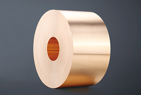
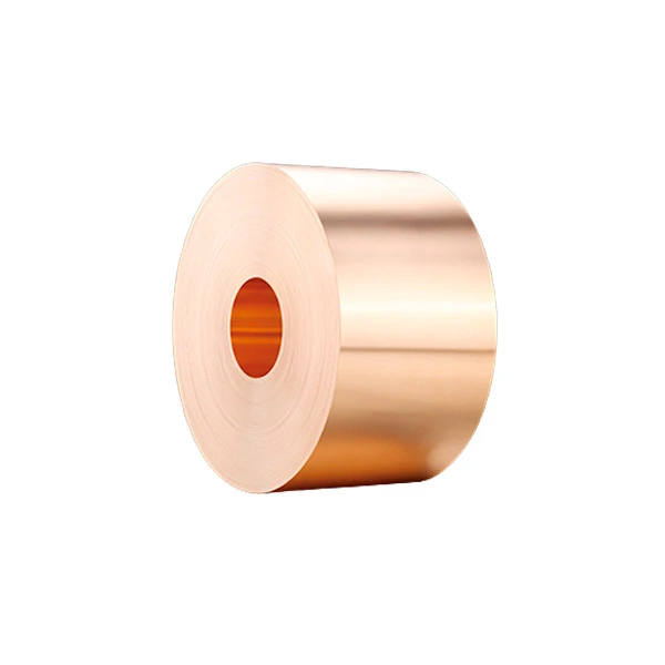
2. Copper Foil
Function: Used as a heat spreader layer in thin devices.
Typical Parameters: Thickness 0.05–0.3mm, can be stamped into complex shapes.
Applications: Back of smartphone SoCs, flexible circuit board heat dissipation.
3. Copper Block
Function: Heat accumulation and diffusion in areas with high heat flux density.
Typical Parameters: Volume 5–50cm³, commonly used in passive cooling designs. Applications: Graphics card VRAM cooling, 5G base station RF modules.
Heat Transfer Components
1. Heat Pipe
Structure: Copper tube shell + sintered copper powder wick + working fluid (water/acetone).
Performance: Effective thermal conductivity can reach 5000–10000 W/(m·K), 10–20 times that of pure copper.
Specifications: Diameter 3–8mm, length 50–300mm (notebooks typically use 5–6mm diameter).
Applications: Laptop cooling modules, server GPU cooling modules.
2. Vapor Chamber
Structure: Flat copper chamber + internal micro-channels/sintered wick, working similarly to heat pipes.
Advantages: 2D heat dissipation, heat spread area is 3–5 times larger than heat pipes.
Typical Dimensions: Thickness 0.4–1.5mm, area 20–100cm² (small vapor chambers for phones can be as thin as 0.3mm).
Applications: High-end smartphones, ultra-thin laptops.
Heat Dissipation Expansion Components
1. Copper Heat Sink Fins
Design: Single fin thickness 0.1–0.3mm, spacing 1–3mm, combined with the base plate through welding or Fin pressing process.
Optimization Direction: Sawtooth/wavelike edge designs increase turbulence, improving convection efficiency by 10–15%.
Applications: Air-cooled heatsinks (e.g., CPU tower coolers), power modules.
2. Copper Radiator
Structure: Copper tubes (φ6–12mm) + aluminum/copper fins, for liquid cooling systems.
Performance: Single rack-level radiator surface area generally needs 6–10m² (40kW cooling demand).
Applications: Data center immersion cooling, high-performance computing (HPC) clusters.
Interface Materials and Composite Components
1. Copper Thermal Pad
Characteristics: Flexible pad filled with copper powder/graphite, thermal conductivity 5–20 W/(m·K).
Advantages: Fills gaps on uneven surfaces (compression rate 20–30%).
Applications: SSD main controller cooling, automotive electronics.
2. Copper-Graphite Composite Material
Ratio: Copper 60–80%, graphite provides anisotropic thermal conductivity.
Performance: In-plane thermal conductivity 400–600 W/(m·K), 40% lighter than pure copper.
Applications: Ultra-thin laptop covers, drone flight controllers.
3. Direct Copper Bonded Substrate (DCB)
Structure: Ceramic (Al₂O₃/AlN) sandwich copper plate, copper layer thickness 0.2–0.5mm.
Characteristics: High voltage resistance (>2kV), low thermal resistance (0.2–0.3 K·cm²/W).
Applications: IGBT modules, electric vehicle inverters.
Components for Liquid Cooling Systems
Copper Cold Plate
Design: Internal microchannels (0.5–2mm wide), ΔP<50kPa at a flow rate of 3–10L/min.
High-performance Model: For AI server GPUs, can handle heat flux densities >100W/cm².
Copper Quick Disconnect Fittings
Requirements: Nickel-plated surface for corrosion resistance, pressure resistance ≥1MPa, leakage rate <1×10⁻⁶ mbar·L/s.
Applications: Data center maintainable liquid cooling circuits.
Special Process Components
Porosity: 50–70%, pore size 10–100μm, specific surface area >0.5m²/g.
Uses: Heat pipe wicks, phase change material (PCM) carriers.
3D Printed Copper Heat Sinks
Process: Selective laser melting (SLM), smallest wall thickness 0.2mm.
Advantages: Topologically optimized structures, surface area 3 times higher than traditional designs.
Applications: Custom server cooling, aerospace electronic equipment.
Plated Copper Heat Dissipation Structures
Component Performance Comparison Table
Characteristic | Copper | Aluminum (reference) |
Thermal Conductivity | 401 W/(m·K) | 237 W/(m·K) |
Melting Point | 1083°C | 660°C |
Typical Processing Techniques | Sintering, die casting, electroplating | Extrusion, die casting |
Cost (relative) | 1.5–2 times that of aluminum | Benchmark |
Suitable Scenarios | High power density areas | Medium to low power devices |
Evolution and Innovation of Copper Heat Dissipation in 3C Products
Copper Heat Dissipation in Smartphones
Modern smartphone heat dissipation has evolved from early graphite sheets to composite heat dissipation solutions. Typical flagship models use a multi-layer structure: the SoC directly contacts copper foil (0.1-0.3mm thick), connected to a copper vapor chamber (0.4-0.6mm thick) through thermal gel, with an outer graphene film enhancing lateral heat dissipation. Measurements show using a copper vapor chamber can decrease the SoC junction temperature by 8-12°C, significantly better than pure graphite solutions. Apple's iPhone 14 Pro's A16 chip adopts a copper alloy heat dissipation frame, reducing thermal resistance by about 15%; while Samsung Galaxy S23 Ultra's vacuum vapor chamber area reaches 2724mm², achieving uniform heat dissipation across the device with a copper mesh structure.
Copper Heat Pipes in Laptops
High-performance laptop cooling systems usually contain 2-4 copper heat pipes with diameters of 5-8mm and wall thicknesses of 0.3-0.5mm. Products like the ROG Zephyrus G14 use 3D vapor chamber technology, combining traditional heat pipes with vapor chambers, achieving a heat flux of 80W/cm². It is worth noting that controlling the porosity of the sintered copper powder wick in the heat pipe at 50-70% achieves optimal balance between capillary and fluid resistance, allowing effective heat transfer distances of 30-50cm. Some manufacturers are experimenting with copper-graphite composite materials, maintaining 85% of copper's thermal conductivity while being 40% lighter.
Copper Heat Dissipation in Miniaturized Devices
Wearable devices, constrained by space, use ultra-thin copper films (thickness <100μm) combined with phase change materials (PCM). The Huawei Watch GT3 Pro uses a 0.08mm copper foil combined with a paraffin material, increasing heat capacity by 30%. TWS earphones generally use copper plating techniques, depositing a 2-5μm copper layer on plastic structures, controlling weight while improving local hotspots. Data shows copper plating can reduce the temperature distribution standard deviation inside the earphone charging case from ±4.2°C to ±1.8°C.
Deep Application of Copper in AI Server Cooling Systems
GPU/CPU Copper Cooling Solutions
The NVIDIA H100 GPU adopts a full-coverage copper cold plate with a contact area of 38cm², a microchannel structure hydraulic diameter of 0.5mm, and a thermal resistance of only 0.08°C/W at a flow rate of 3-5L/min. The AMD EPYC 9654 processor's cooler uses copper base welding, with a base thickness of 8mm, having 68% higher heat diffusion efficiency than aluminum materials. In liquid cooling systems, the design of copper cold plate flow channels is particularly critical: staggered fin structures (spacing 1.5mm, height 5mm) can increase the Nusselt number to 1.8 times that of conventional designs.
Copper Applications in Rack-Level Liquid Cooling
Immersion liquid cooling uses copper pipes with purity >99.9%, wall thickness 1.5-2mm to resist fluorine liquid corrosion. For a 40kW cooling demand per rack, the copper radiator surface area needs to reach 6-8m², maintaining ΔT<15°C with a wind speed of 0.3m/s. Google TPU v4 racks use copper-aluminum composite heat sinks, achieving optimal cost-performance with 60% copper ratio, and a thermal resistance coefficient of 0.0045m²·K/W. It's important to control the electrochemical corrosion rate of copper in dielectric fluids to <5μm/year, requiring strict surface passivation treatments.
Power Modules Copper Cooling
In 80Plus Titanium certified power supplies, copper heat sinks account for 15-20% of the total weight. GaN devices use directly copper bonded (DCB) substrates, with a copper layer thickness of 0.3mm and a thermal resistance as low as 0.24 K·cm²/W. In three-phase rectifier modules, the copper busbar cross-sectional area correlates with current: 25mm² per 100A, keeping temperature rise within 40K. Server power supply copper heat sinks usually undergo micro-arc oxidation treatments to form a 10-20μm ceramic layer, maintaining thermal conductivity while increasing voltage resistance to over 3kV.
Challenges and Innovation Directions for Copper Heat Dissipation
Weight and Cost Optimization
Copper's density (8.96g/cm³) is 3.3 times that of aluminum, becoming a noticeable drawback in mobile devices. New copper alloys such as C7025 (2.5% Ni-0.65% Si) maintain 85% of the thermal conductivity while increasing strength to 450MPa. Porous copper materials (porosity 50-70%) can achieve densities of 1.8-2.5g/cm³, with thermal conductivities still reaching 150-200 W/(m·K). Cost-wise, copper recycling technology can improve material reuse rates to 95%, saving 85% energy compared to primary copper.
Advanced Manufacturing Processes
3D-printed copper heat sinks have achieved wall thicknesses as small as 0.2mm, with complex internal structures increasing the surface area by 3-5 times. Selective laser melting (SLM) formed copper heat sinks, demonstrate 20% lower thermal resistance under a heat flux of 50W/cm² compared to traditional processing. Nano copper sintering technology can achieve joint thermal resistances of <5mm²·K/W at low temperatures of 250°C, particularly suitable for chiplet packaging. Micro-injection molding technology can manufacture 100μm-level copper micro-pin arrays, with boiling heat transfer coefficients reaching 100kW/(m²·K).
Heterogeneous Material Integration
Copper-diamond composite materials (containing 50vol% diamond) have thermal conductivities of 600W/(m·K), but their cost limits commercial use. Graphene-enhanced copper matrix composites, with 1wt% addition, increase thermal conductivity by 25%, with adjustable CTE matching the chip. Recently developed copper-carbon nanotube vertical arrays have axial thermal conductivities exceeding 800W/(m·K), potentially useful for 3D IC cooling. It is important to note that interface thermal resistance remains a major challenge, with molecular-level bonding techniques potentially reducing interface thermal resistance to <10mm²·K/W.
Conclusion
Copper's fundamental advantages as a heat dissipation material are difficult to completely replace, but its application forms will continue to evolve. Driven by the dual trends of thinner 3C devices and the increasing power density of AI servers, copper in the heat dissipation field is progressing towards heterogeneous integration, intelligent control, and nano-structuring. In the next decade, we may witness a leap from "quantitative change" to "qualitative change" in copper's role in thermal management.

 English
 한국어
한국어 français
 Deutsch
 Español
 italiano
 العربية
 tiếng việt
 Türkçe
 ไทย
ไทย 中文
中文

