With the continuous development of emerging products and applications such as artificial intelligence, 5G, Internet of Things, smart manufacturing, and new energy vehicles, the conductor packaging material market is also continuously evolving. The demand for diversified, lightweight, small-sized, and intelligent terminal devices has prompted packaging materials, including lead frames, to continuously evolve towards high density, high reliability, high heat dissipation, low power consumption, and low cost.

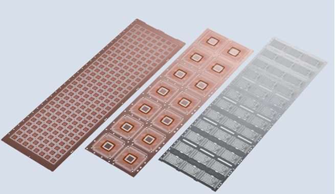
Figure: Lead Frame, Source: Sunlight Electric
The lead frame industry is a technology-intensive and capital-intensive industry, and production bases are mainly concentrated in the Yangtze River Delta and the Pearl River Delta. Foreign-funded enterprises and domestic enterprises each account for 50% of the Chinese market.
Compared to foreign countries, due to the late start and weak foundation of domestic etching lead frame companies, production equipment, products, and technical processes are relatively backward, leading to the dominance of the domestic high-end market by foreign-funded enterprises. In terms of technology, the products of domestic lead frame production companies are mainly focused on stamped lead frames, and the proportion of etched lead frames is still very small. Nowadays, many domestic companies have increased their investment in lead frame research and development, and domestic substitution is in full swing.
So, What Is a Lead Frame?
A lead frame, as a chip carrier for integrated circuits, is a key structural component that uses bonding materials to realize electrical connections between the internal circuit leads of the chip and external leads, forming an electrical loop. It serves as a bridge connecting external wires and is an important basic material in the electronic information industry.
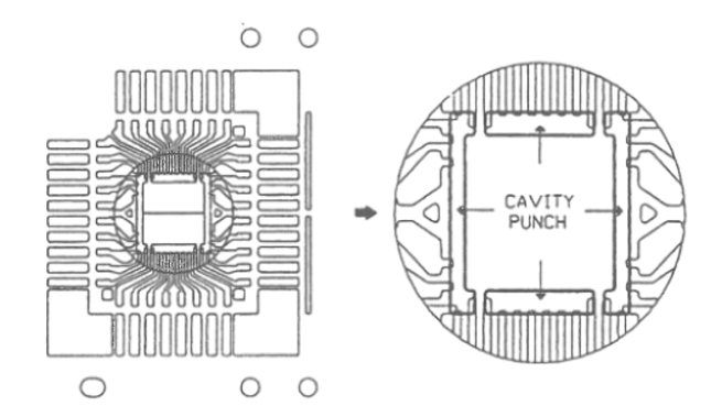
The lead frame consists of chip pads and pins. The chip pads provide mechanical support for the chip during the packaging process, while the pins connect the chip to the external electrical circuitry. Each pin terminal is connected to a pad on the chip through a lead, and this terminal is called an inner pin, while the other end of the pin is called an outer pin, which provides mechanical and electrical connections to the substrate or PCB.
The Functions of a Lead Frame
Providing support for packaging devices
Preventing the sudden overflow of molding material between leads and providing support for the plastic
Connecting the chip to the substrate, providing electrical and thermal channels between the chip and the circuit board
The functional requirements of a lead frame require the lead frame materials to meet the following characteristics:
Good thermal and electrical conductivity, which can reduce the adverse effects caused by capacitance and inductance, and is also conducive to heat dissipation
Low coefficient of thermal expansion, good matching, solderability, corrosion resistance, thermal resistance, oxidation resistance, and good plating properties
Sufficient strength, rigidity, and formability. The tensile strength is generally greater than 450 MPa, and the elongation is greater than 4%
Good flatness and small residual stress
Easy to process without burrs
Low cost, meeting the requirements of large-scale commercial applications
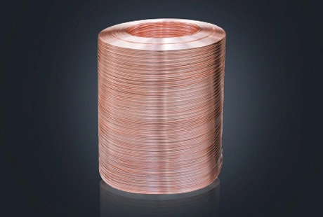
Lead frame copper tape is one of the main raw materials for lead frames. Currently, Jintian Copper produces grades such as C1921, C1920, and C7025.
The Processing Methods of Lead Frame
Stamping method
Etching method
Stamping Method
Mechanical stamping method generally uses stepping tools to perform cutting through mechanical force. The molds used in this method are expensive, but the production cost of the frames is low.

Etching Method
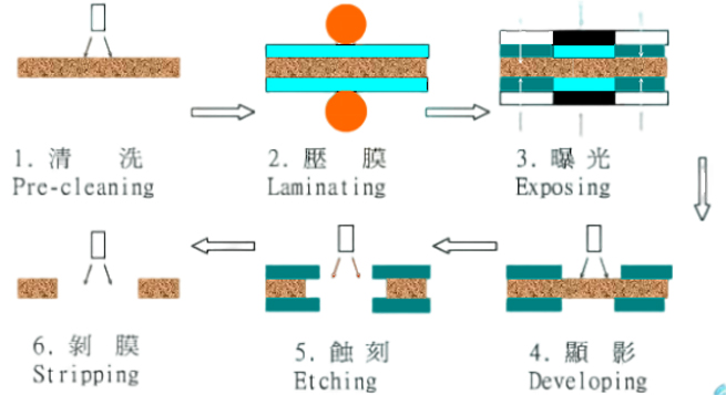
For frames used in micro-spacing packaging, etching method is usually used because the precision of mechanical stamping processing cannot meet the requirements of high-density packaging. The chemical etching method can be roughly divided into the following 5 steps:
Stamping positioning holes
Double-sided coating and polishing glue
UV exposure, development, and curing through mask plate
Expose metal by corrosive chemicals (usually using ferric chloride and other reagents)
Remove photoresist

Jintian Copper was established in 1986 and has been focusing on the copper processing field for over 30 years. Its main products include various high-precision tin-phosphorus bronze strips, brass strips, bronze strips, zinc brass strips, copper-nickel silicon bronze strips, and lead frame copper strips.
If you have any related demand for copper alloy strip products, please contact Jintian at 83005999. We look forward to your call!

 English
 한국어
한국어 français
 Deutsch
 Español
 italiano
 العربية
 tiếng việt
 Türkçe
 ไทย
ไทย 中文
中文
